CALICE-UK ECAL Prototype Readout Electronics
Contains links, documents, etc., for the CALICE-UK prototype ECAL electronics
- Project overview
- Project specification
(ps,
pdf)
- Schedule:
overall and prototype tests (ppt),
VFE tests (pdf)
- RAL ID
website,
containing links to the Quality Management System information
- Reviews
- External interfaces and requirements
- ECAL: VFE-PCB
(ps,
pdf),
connector schematic:
(ps),
application notes
(FLC_PHY2: doc,
FLC_PHY3: doc,
PCB V2:
interface doc,
test assembly doc,
bug report doc),
VFE PCB V2 schematics
(ps; all, pages
1
2
3
4
5
6
7
8
9
10),
photos
(dir)
- AHCAL:
HAB manual V4
(pdf),
slow controls interface
(pdf)
- DHCALE:
HaRDROC
home page
and configuration data list
(txt),
datasheet
(pdf),
DHCAL1 board SCSI interface
(xls)

- Trigger inputs
(doc,
pdf)
- Data Acquisition
(ps,
pdf)
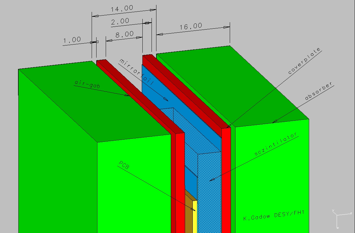
- Mechanical:
ECAL scanning table
details
(doc),
readout
(doc),
data structure
(pdf),
HCAL scanning table
(jpg, 1, 2)
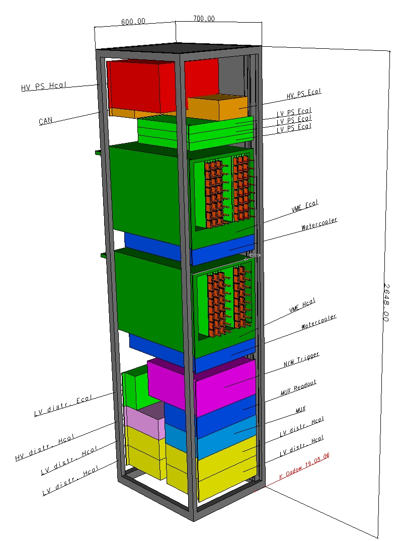
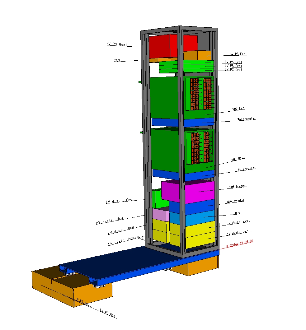
- CERN rack layouts
(jpg, 1,
2),
cable runs
(pdf)
- System
- Readout board
- Overview
(ps,
pdf),
data paths
(pdf)
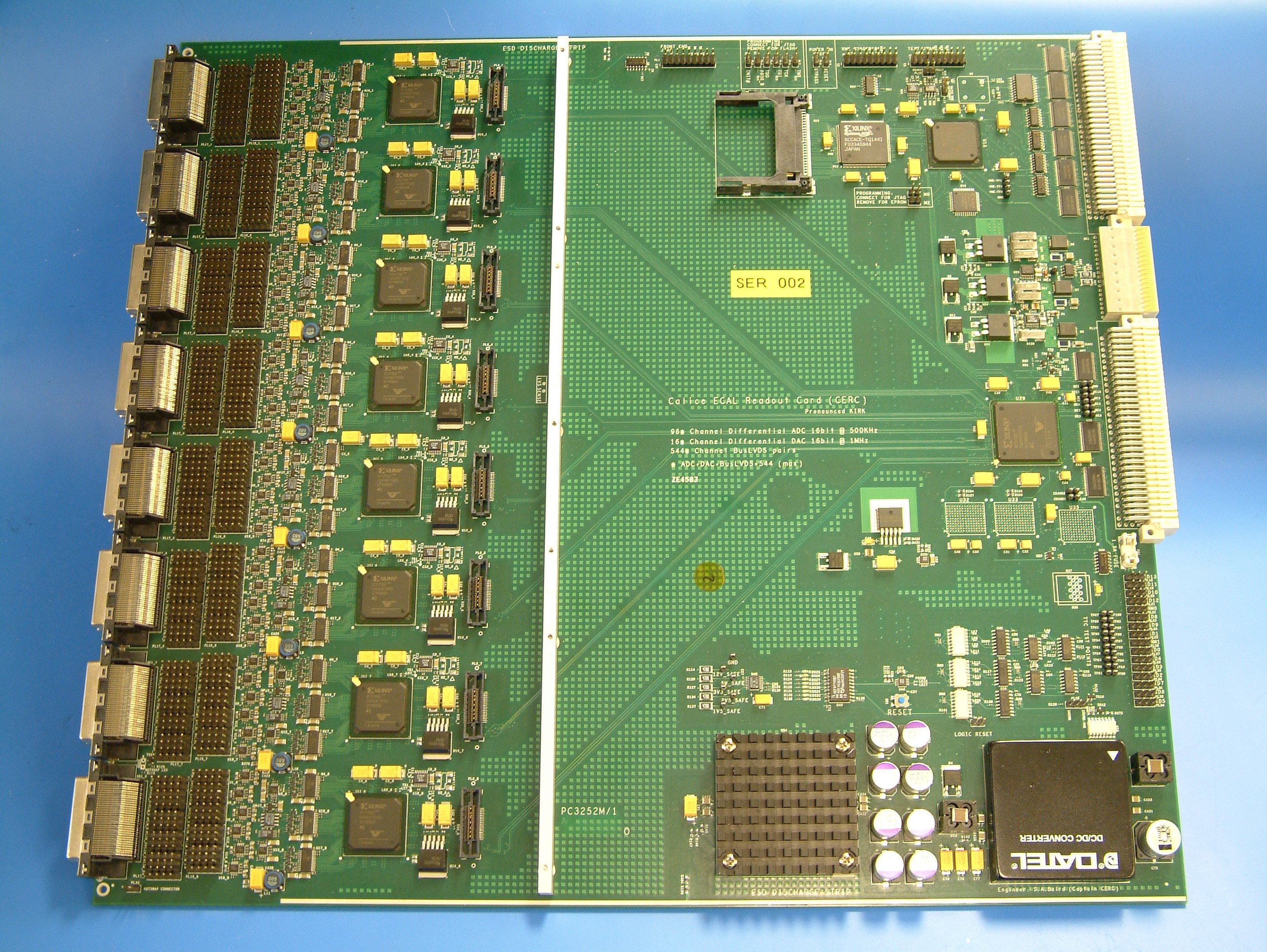
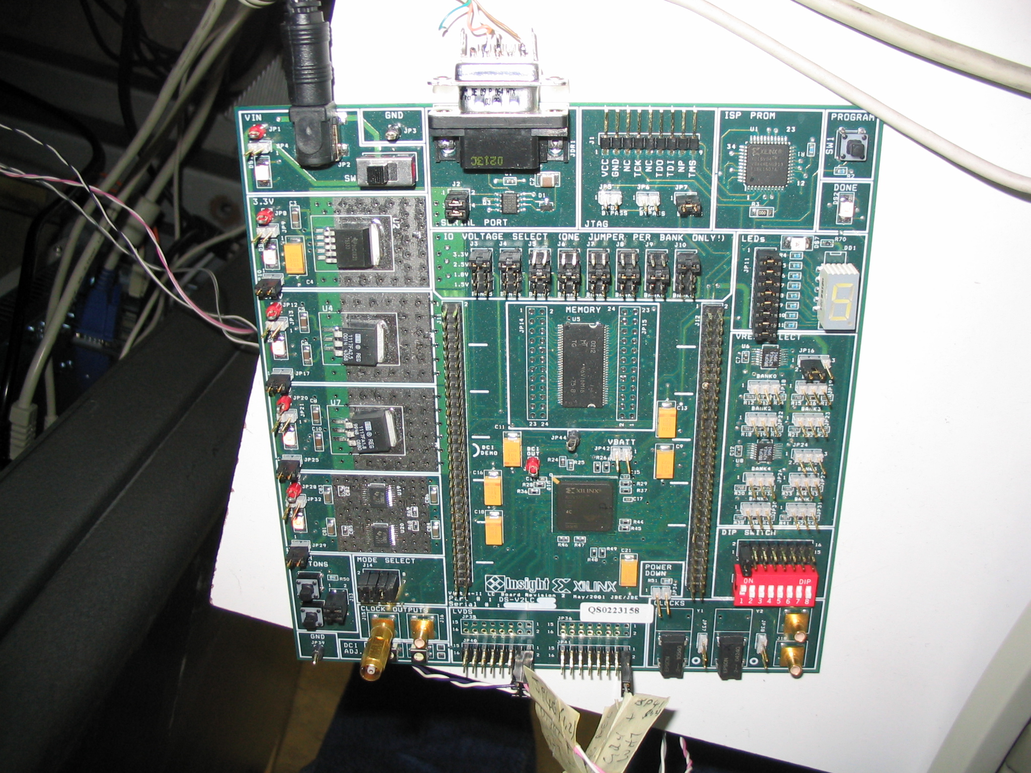
- Prototype photo
(tif,
jpg)
- External interface: VFE-PCB (see above),
front panel layout
(ppt,
pdf),
cable connectors:
html
- External interface: VME
(pdf)
- Prototype technical information
web page,
schematics
(pdf)
- User guide linked from Adam's
website
- Firmware:
VME
(dir),
BE
(dir),
FE
(dir)
CompactFlash
(dir)
- Internal interface: master-to-slave FPGA configuration path timing
(pdf)
- Internal interface: slave-to-master FPGA data path
(ps,
pdf)
- Master FPGA: FPGA block diagram
(pdf),
pin estimate
(txt)
- Slave FPGA: FPGA block diagram, pin estimate and ADC control timing
(ps,
pdf),
missing Fig 1
(doc,
ps)
- Proposed FPGA's (Virtex-II),
System ACE (pdf)
- Proposed ADC: TI ADC's
overview,
ADS8361
- Proposed DAC:
AD5541
- Slow controls monitoring:
voltages
ADM1025A
(pdf),
temperature
LM82
(pdf)
- EPROM board id: X24165
(pdf)
- Cost estimate
(xls)
- Problem reports
website
- Front End FPGA
- Block diagram: front end
(ps,
pdf)
- Back End FPGA
- Block diagram: back end
(ps,
pdf)
- Trigger
- Block diagram: trigger section of back end
(ps,
pdf)
- Block diagram
(ppt,
pdf),
functional diagram
(ppt,
pdf),
description
(doc,
pdf)
- External interface: inputs (see above),
front panel layout
(ppt,
pdf)
- External interface: VME
(doc,
pdf)
- Test board
- Block diagram
(ps),
functional diagram
(ppt,
pdf)
- External interface: VFE-PCB (see above),
front panel layout
(ppt,
pdf)
- External interface: VME (see above)
- RS232 System
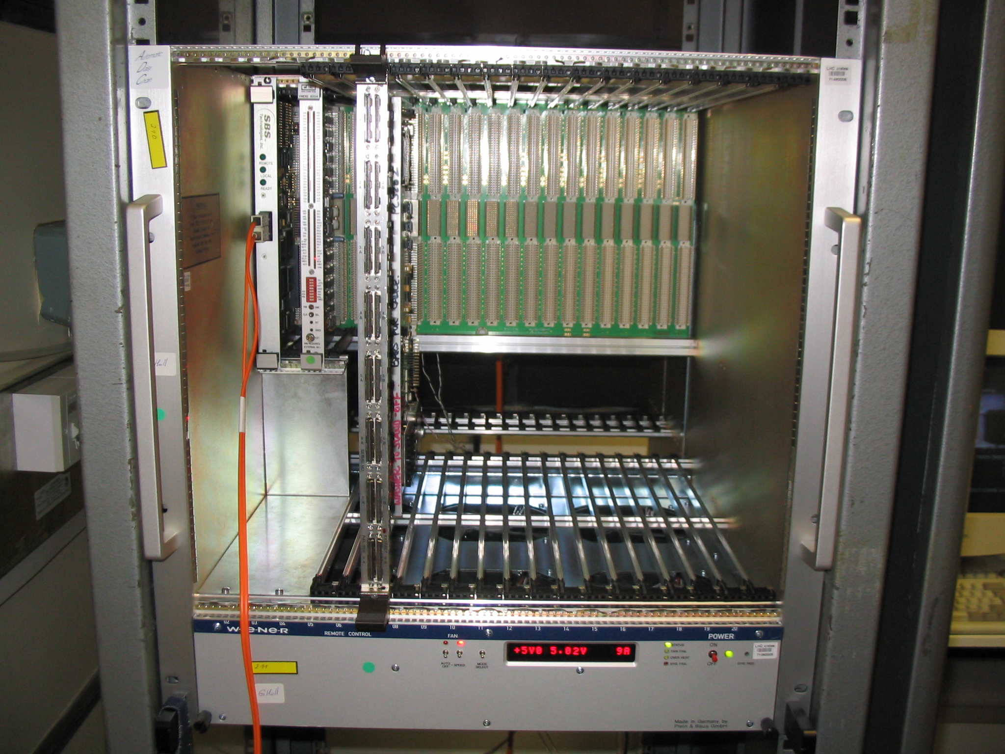
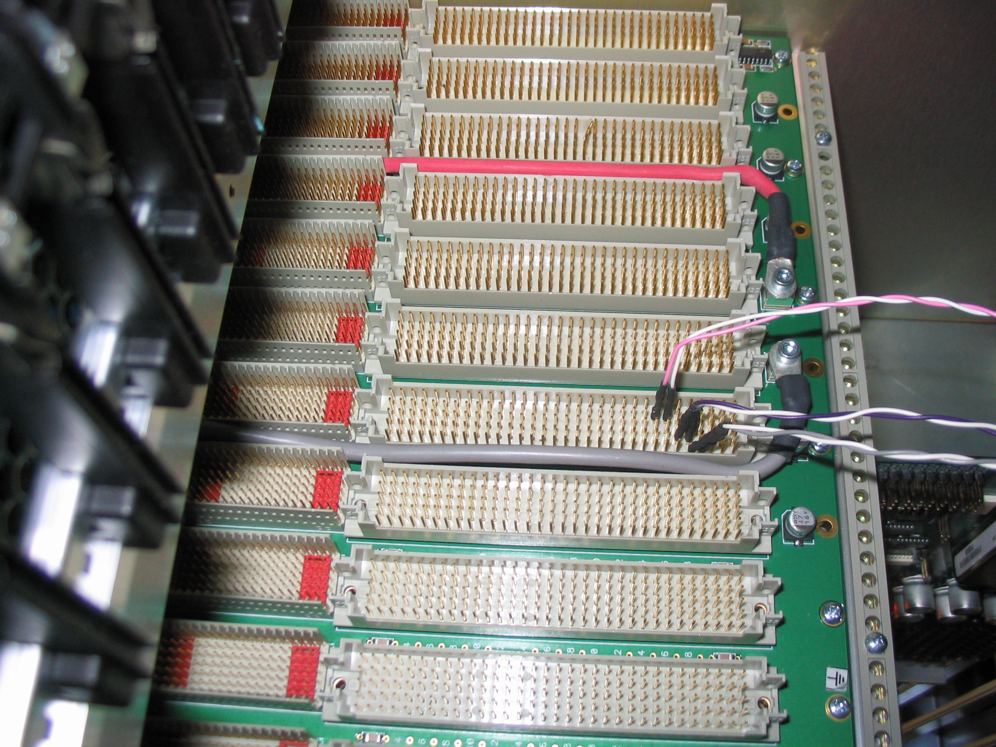
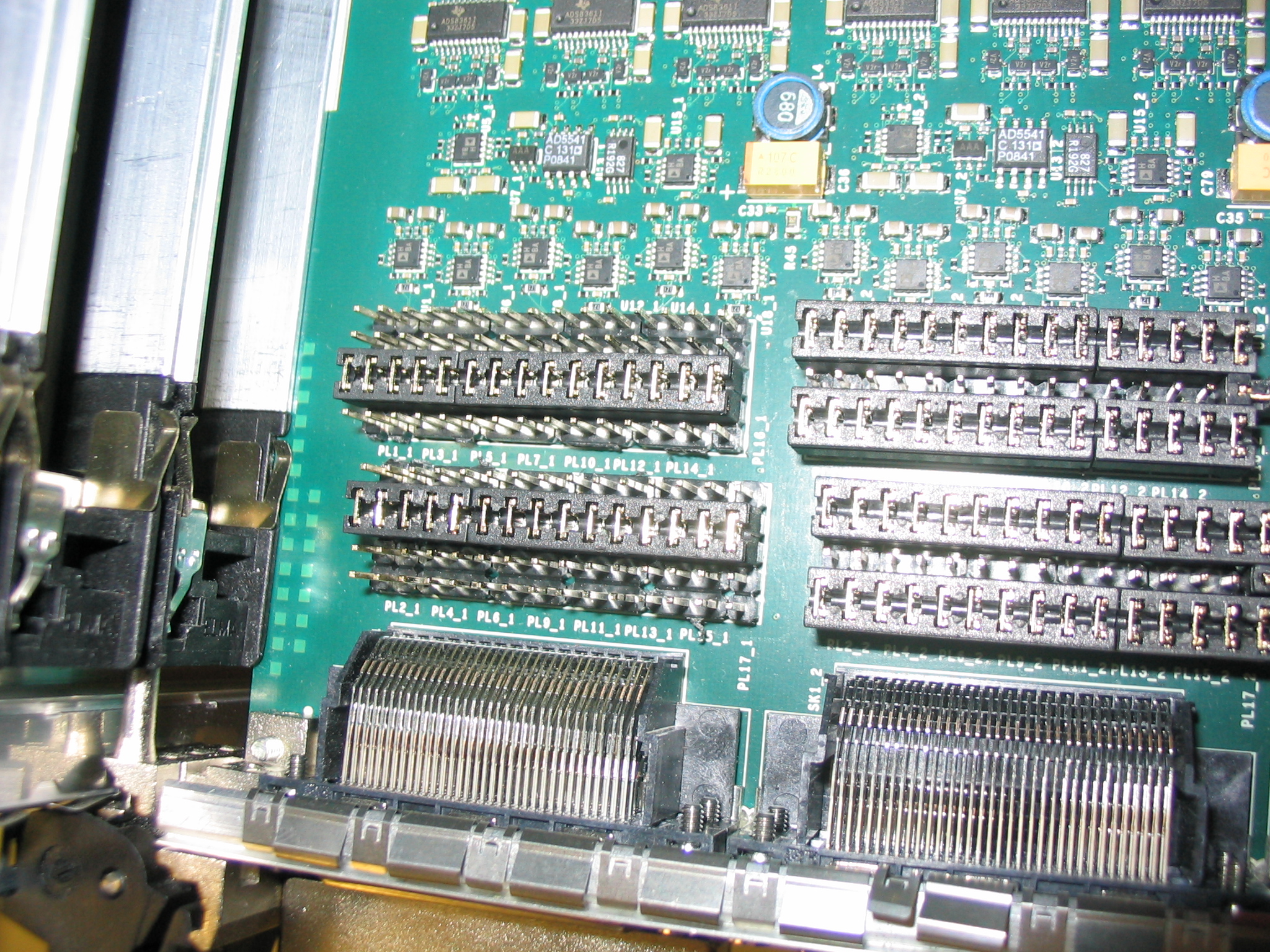
- Photos:
front of crate (jpg),
back of crate (jpg),
CERC link array (jpg),
development board (jpg),
VFE PCB (jpg)
- Software
- CERN Hardware Access Library (HAL)
web page
- CMS FED HAL memory map file (dat)
- Related links
- File access
Go to the CALICE-UK home page